Hardware
Dimensions
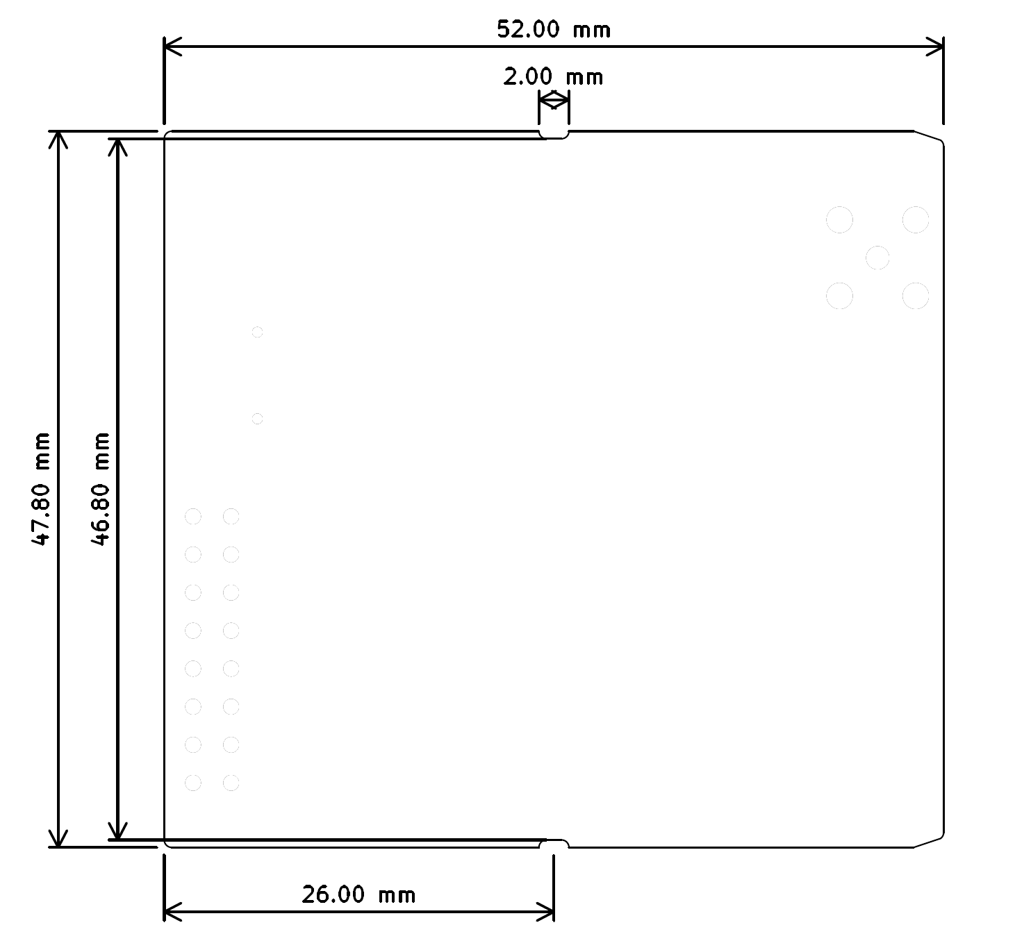
RockBLOCK 9704-SMA Dimensions
RockBLOCK 9704-ANT Dimensions
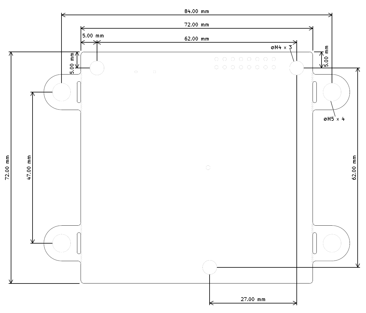
CAD data is available to download at the bottom of the page.
Initial Connection
DC Input
The red 'PWR' LED should illuminate, and the supercaps will begin charging. With the default current limit, this can take around 40 seconds. The 9704 module will start up, and the the Green 'RDY' LED should illuminate.
Battery Input
The red LED will not illuminate. The onboard supercaps will begin charging. With the default current limit, this can take around 25 seconds. The 9704 module will start up, and the the Green 'RDY' LED should illuminate.
USB Input
The red 'PWR' LED should illuminate, and the supercaps will begin charging. With the default current limit, this can take around 40 seconds. The 9704 module will start up, and the the Green 'RDY' LED should illuminate. Please note that the USB-TTL device will not enumerate until the Green LED illuminates.
If using USB, the RockBLOCK 9704 should be plugged directly into a USB 2.0 or USB 3.X port, which must be able to supply 500mA. For this reason, the use of unpowered USB hubs is not supported.
If using DC or USB input, and the Green LED doesn't illuminate, there could be residual charge on V_BATT, preventing the onboard supercap charger from operating. This can be remedied by grounding V_BATT.
Communication
RockBLOCK 9704 has an FTDI USB-TTL interface for quick and easy communication, or a 16-pin 0.1" pitch interface for full control and the highest efficiency capability. We have tested USB cables and extenders up to 6m in length with no problems, however any USB cable used should be of good quality to minimise voltage drop and maximise signal integrity.
The USB-TTL interface and the 16-pin connector share a serial interface on the 9704.
Simultaneous connection of both interfaces may cause damage to the RockBLOCK 9704.
It is important to note that the 9704 has some requirements surrounding startup and shutdown sequencing.
1. Using 16-pin connector:
Startup Sequence
- Set all pins† connected to RockBLOCK 9704 inputs tristate (high-Z) or logic low.
- Apply Power to RockBLOCK 9704
- Tristate / Logic High / Pull-up I_EN
- Wait for I_BTD to go HIGH
- UART / input pins can now be initialised.
Shutdown Sequence
- Cease serial communications
- Drive I_EN LOW
- Wait for I_BTD to go LOW
- Set all pins† connected to RockBLOCK 9704 inputs tristate (high-Z) or logic low.
- Power may be removed at this point if desired.
† Pin 5 - GPS_EN is exempt from this requirement.
When not booted, the output states of the RockBLOCK 9704, with the exception of I_BTD, are to be considered undefined.
2. Using USB:
Startup Sequence
- Connect RockBLOCK 9704 to a USB port
- Sequencing is handled in hardware
- USB port will enumerate on the host device once the 9704 has booted successfully.
Shutdown Sequence
- Unplug / power down the USB port
- The module will automatically shut down on capacitor power.
It is important that the 9704 is allowed to complete a startup / shutdown cycle. Therefore, once the I_EN has been driven high, the host application must wait for I_BTD to transistion high before driving I_EN low again.
Vice-versa, once I_EN has been driven low, the host application must wait for I_BTD to transistion low before driving I_EN high again.
Failure to follow this procedure may result in damage to the 9704 module.
Connections
RockBLOCK 9704 Connector Pinout
PCB version 2A onwards
| Pin | Label | Function | Type | Direction |
|---|---|---|---|---|
| 1 | GND | Signal Ground | GND | GND |
| 2 | I_SYN | Iridium SYNC_XCVR_OUT | Logic | OUT |
| 3 | I_EN | Iridium Enable | Logic | IN |
| 4 | GND | Signal Ground | GND | GND |
| 5 | GPS_EN | GNSS Passthrough Enable Signal | Logic | IN |
| 6 | P_EN | Cap Charge Enable Signal (ACTIVE LOW) | Logic | IN |
| 7 | I_BTD | BOOTED signal from 9704 module | Logic | OUT |
| 8 | XMT_G | XMIT_GATE high when actively transmitting | Logic | IN |
| 9 | I_WK_I | WAKE_XCVR_IN to wake 9704 from host circuit | Logic | IN |
| 10 | GND | Signal Ground | GND | GND |
| 11 | I_WK_O | WAKE_XCVR_OUT to wake host circuit from 9704 | Logic | OUT |
| 12 | V_BATT | Power Input (3.6-4.5V @ 1.1A) | Power | IN |
| 13 | TXD | UART_XCVR_TX data FROM 9704 to host circuit | Logic | OUT |
| 14 | RXD | UART_XCVR_RX data TO 9704 from host circuit | Logic | IN |
| 15 | V_IN+ | Power Input (4.0-5.3V @ 500mA) | Power | IN |
| 16 | V_IN- | Power Ground | GND | GND |
- Pin directions are relative to the RockBLOCK 9704. For example:
- I_EN is an INPUT which means it must be driven by the host circuit into the RockBLOCK 9704.
- I_BTD is an OUTPUT which means the RockBLOCK 9704 will drive HIGH or LOW into the host circuit.
- I_EN is an INPUT which means it must be driven by the host circuit into the RockBLOCK 9704.
Signal Thresholds
The host circuit should be compatible with the following I/O voltages to ensure trouble-free operation of the RockBLOCK 9704.
| RB9704 Pin | V Min. | V Max. | I Max. (mA) |
|---|---|---|---|
| DC Power | 4.0 | 5.3 | 500 |
| Battery Power | 3.6 | 4.5 | 1100 |
| Logic In LOW | -0.3 | 0.4 | -0.2 |
| Logic In HIGH | 2.0 | 3.6 | 0.2 |
| Logic Out LOW | 0 | 0.4 | -2 |
| Logic Out HIGH | 2.9 | 3.4 | 2 |
Pin Descriptions
1, 4, 10, 16 - GND / V_IN-
These are signal ground pins. All should be connected to the host circuit, unless used in USB only mode.
2 - I_SYN
The SYNC_XCVR_OUT signal is intended for use in RF test cases such as regulatory approvals, and is inactive in operational states. This pin can be left open.
3 - I_EN
This input pin is used to initiate startup and shutdown of the 9704 module. The signal is buffered into the ENABLE input of the 9704 module. It has a weak voltage-divider (270KΩ/430KΩ) pull-up to the input voltage, ensuring that the 9704 Boots up when powered on, and begins shutting down as soon as external power is removed. This pin has a series 10KΩ resistor to the input of the buffer. It can be driven directly with an MCU pin, or an open-drain output.
5 - GPS_EN
This input pin is connected directly to the 9704. When driven high, it enables the RF path between the Iridium antenna (Patch or SMA) and the U.FL 'GNSS' connector. This path can still be enabled if the 9704 is shut down, however the power supply must still be connected and enabled (P_EN driven low or left open). Isolation of the 'GNSS' connector during a transmit burst from the 9704 is handled directly by the 9704 itself. This pin can be left open or driven low if not required.
6 - P_EN
This input pin is used to enable or disable the Supercapacitor charge circuit. It has a weak pulldown of ~1MΩ. Leaving open or driving LOW enables the charge circuit. Driving high disables the charge circuit.
7 - I_BTD
This output pin signals when the 9704 is booted (high) or shut down (low). When this pin is LOW there should be no voltage applied to any input pins, other than I_EN which will cause the 9704 to boot if driven high. The state of this pin is used onboard the RockBLOCK 9704 to control the 'RDY' LED, and the operational status of the USB-TTL bridge (when on USB power only).
8 - XMT_G
The XMIT_GATE output pin drives HIGH when 9704 is actively transmitting. The default lead-and-lag time of this pin is 1µS, but can be controlled in software for specific host requirements. This pin also controls the onboard 'XMT' LED. If unused, it can be left open.
9 - I_WK_I
The WAKE_XCVR_IN input pin allows host and 9704 power control. When driven low, it tells the 9704 that it can sleep. When driven high, it instructs the 9704 to wake. I_WK_O shows the 9704's response. Wake functionality must be enabled in software. This pin can be left open if not required.
11 - I_WK_O
The WAKE_XCVR_OUT output pin allows host and 9704 power control. When I_WK_I is driven high, the 9704 wakes, and drives I_WK_O high to signal it's ready to send an MO message. Alternatively, when an unsolicited MT message is received, this pin is driven high. Once the Host responds by driving I_WK_I high, the 9704 sends the message out over UART. Wake functionality must be enabled in software. This pin can be left open if not required.
12 - V_BATT
This is the battery power input pin for RockBLOCK 9704. It requires a voltage between 3.6V and 4.5VDC, at a maximum of 1100mA. This pin can be used for regulated voltage or single-cell li-ion battery input. It is diode-ored with the DC input voltage. If P_EN is left open, connection of a battery will disable the DC supercap charger to save power. If the P_EN pin IS driven LOW, the onboard DC supply will provide the majority of power to the circuit. Whilst the battery and DC supplies are diode ored, it is recommended that only one power source is connected. Whilst a Lithium battery can provide power, RockBLOCK 9704 does not have a battery charger onboard. Therefore if one is required, it must be included on the host circuit. This pin has NO reverse polarity protection.
PLEASE NOTE In scenarios where only the USB connection is used for power and communications, it is recommended that the V_BATT pin is grounded.
13 - TXD
The UART_XCVR_TX output pin is the Serial Transmit line of the 9704.
14 - RXD
The UART_XCVR_RX input pin is the Serial Receive line of the 9704. NOTE: When connected to USB, this pin is driven by the FT234XD.
15 - V_IN+
This is the DC power input pin for RockBLOCK 9704. It requires a voltage between 4.0V and 5.3VDC, at a maximum of 500mA. This pin can be used for regulated voltage input. It is reverse-polarity protected, and diode-ored with the USB input voltage. If both USB and V_IN+ are connected, V_IN+ will be prioritised, as long as it is above 3.6V.
GNSS Passthrough
The RockBLOCK 9704 has a labelled U.FL connector, which allows the onboard Patch antenna or SMA antenna connection to pass through a signal to the user's GNSS receiver.
Driving Pin 5 - GPS_EN high will enable this passthrough function. Gating of this signal is handled by the 9704 module, preventing damage to the GNSS receiver during Iridium Transmit bursts. Ground Control has sucessfully tested this feature using the uBlox MAX-M10S GNSS receiver, but other receivers should also work.
Please note that power must be supplied to the RockBLOCK 9704 in order for this feature to work. Enabling this feature will add approximately 25mW to the idle power consumption.
GNSS Receivers with Active Antenna Control
Some GNSS receivers place a DC bias on the antenna RF signal line for antenna power and control. The 9704 AC-couples the GNSS_RF_OUT signal to it's internal RF front-end, so it is not possible to power or enable the GNSS passthrough path in the transceiver with this signal.
The following diagram may be used as a guide to enable the 9704 passthrough using the DC component of the GNSS active antenna control.
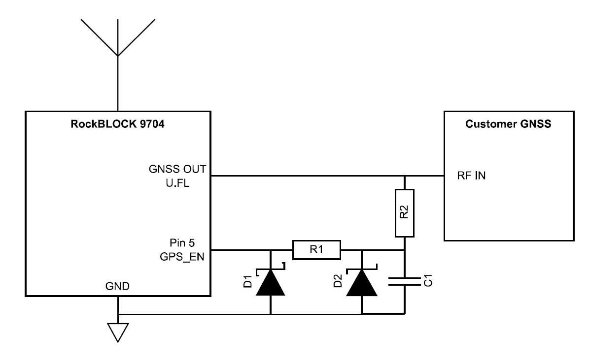 Component values shown are a guide only. Correct values will need to be calculated and prototyped for each specific use case.
| Component | Guide Value |
|---|---|
| C1 | 22pF |
| D1 | >10Vr |
| D2 | 3.0Vbr |
| R1 | 1KΩ |
| R2 | 10KΩ |
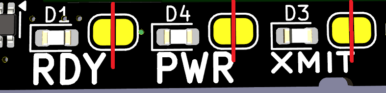
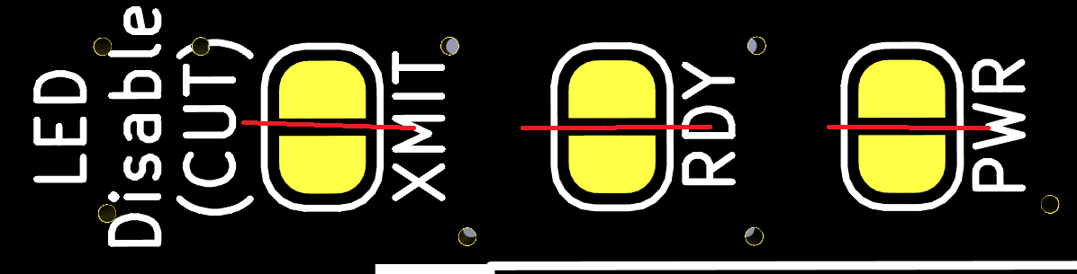
LED Indicators
| Label | Colour | Indication | Power |
|---|---|---|---|
| PWR | Red | ORed input voltage is present | 2.6mW |
| RDY | Green | 9704 Module is powered and booted | 4.6mW |
| XMT | Blue | Modem is actively transmitting | 1.7mW* |
*It is worth noting that this power is consumed only whilst actively transmitting, so will contribute negligibly to overall power use.
Some customers may be keen to save as much power as possible. In order to achieve this, each LED can be individually disabled, using cuttable traces on the board. To re-enable the LED's, the pads can be bridged with a blob of solder.
LED Disable Pads - RB9704-SMA
LED Disable Pads - RB9704-ANT
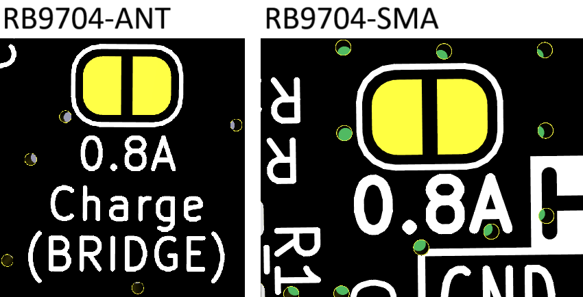
Charge Current
The default DC input charge current of the supercapacitors is limited to ~460mA, to enable the RockBLOCK 9704 to be powered from any USB 2.0 port. This current limit also applies to the 16-pin input.
If the USB connection will be unused, or used soley with USB 3.X ports, the charge current limit can be increased to ~800mA.
To Increase the charge current, the solder pads shown below should be bridged with solder.
The default current limit of the battery input is ~1000mA. This is not designed to be altered.
The default current limit is adequate for constant usage of the RockBLOCK 9704. The only benefit to increasing the current limit is the shortenning of the initial capacitor charge time.
If power to the unit is never removed or disabled, then the increased current limit will have no effect on the operation of the RockBLOCK 9704.
Charge Current Increase Pads
The RockBLOCK 9704 will not negotiate a lower current limit. If a unit with 800mA current limit is plugged into a USB 2.0 port, the port is likely to be damaged!
Downloads
Circuit Diagrams
Schematic - RockBLOCK 9704-SMA (2A1)
Schematic - RockBLOCK 9704-ANT (2A1)
CAD data
STEP - RockBLOCK 9704-SMA (2A)
STEP - RockBLOCK 9704-ANT (2A)
STEP - Mount for RockBLOCK 9704-SMA (RevA)
These documents are intended to provide early access information to interested parties during the development process. Whilst we strive to maintain accuracy, any part of the specification or design of these products may change without notice.
These documents were last reviewed for accuracy on May 1st 2025.